Schematic Diagrams
Notes on the diagram
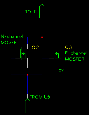 |
| How Q2 and Q3 form an inverter on the PCB |
- Q2 and Q3 are shown as an inverter gate for clarity.
It's not a 7404, it's actually a P and N channel MOSFET. See the
PCB layout for how these are connected.
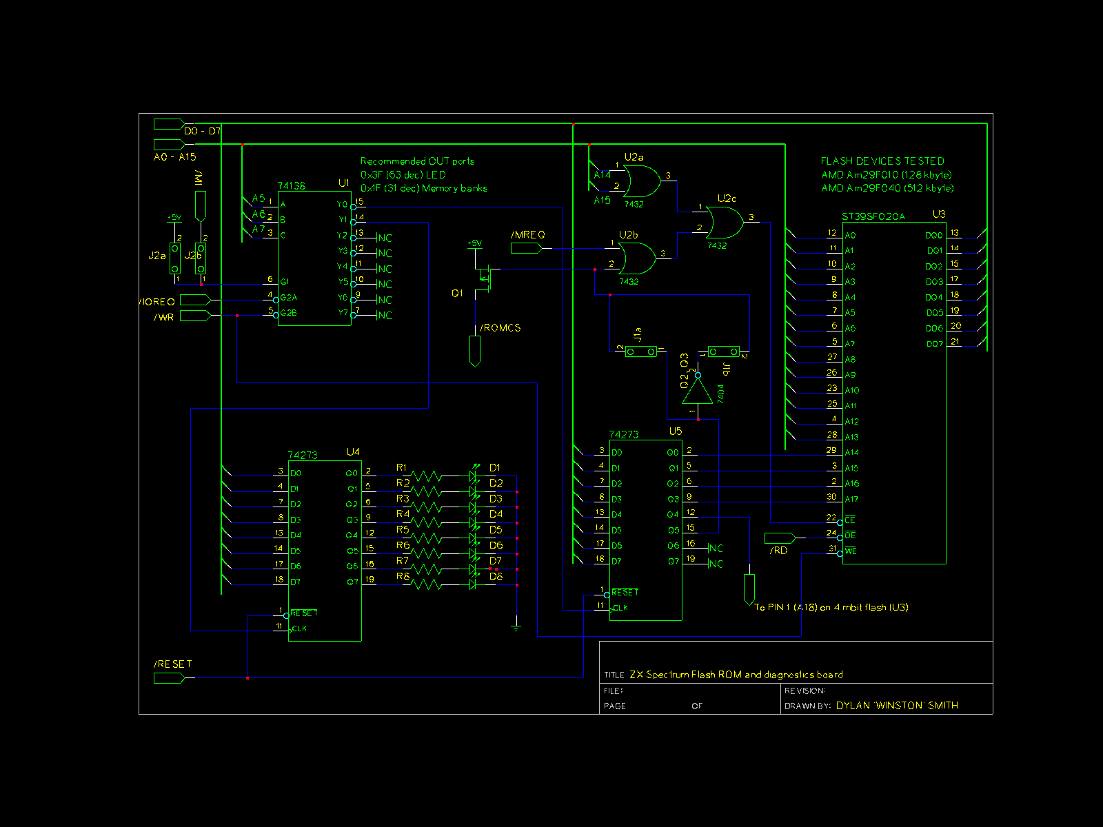
- Due to not having a symbol for a 512K flash chip, a 256K
one is shown in the diagram (and I was too lazy to create one!)
There's a note on the schematic on connecting the final pin.
- The schematic is kind of the 'ideal' as far as pin layouts to
the two 74HC273 chips is concerned. Board layout constraints meant
that on the actual PCB layout, the data lines ended up going to
the easiest-to-route inputs. If you're using the schematic
to build the board on strip board, then this is probably irrelevant
to you since you'll likely be building this with point-to-point
wiring, and so can wire it exactly as shown on the schematic.
If you're looking at the PCB layout, I recommend you
get the datasheet to the '273 to see how the routing works.
- The jumpers used on the PCB layout are 3 pin blocks rather
than two 2 pin blocks.
- On the PCB layout at this site, I used LEDs with built
in resistors, so the discrete resistors showed on the schematic
are not present
Get the schematic
The tool used for this is gSchem, part of gEDA. If you are running
Linux, it's highly likely that gSchem is in your distro's repository -
on Fedora, it's just a matter of using Applications -> Add and
Remove Software, and then selecting it from the list of applications
(use the Search facility to look for 'gschem').
It'll be automatically downloaded (bizarrely, it ends up in
'Edutainment' on the Gnome menu - don't ask me why!) It can also
be started by typing 'gschem' in the shell as well.
gSchem downloads for other platforms can be found at the
gEDA website
Subsitutions
See the Components page for some
component subsitution and omissions suggestions. For example,
the inverter formed by Q2 and Q3 can be replaced by a single
N-channel MOSFET and a 1K resistor if you're making the board
on strip board and don't fancy trying to solder SOT-23 packages.
Q1 can be replaced by a bipolar NPN transistor and base resistor
too.
[Back]