First things first: the Spectrum just isn't hot pluggable. To avoid killing your machine even harder (or killing a working machine if you're making other uses of the board), make sure you do the following before plugging the board into the Spectrum. This may seem like old hat, but just some reminders:
The board is very simple to use. For diagnostics work, check that:
The reason for jumpering out the M1 signal is that if you have a machine that has a Z80 with a poorly functioning M1 line, the board won't work properly. Normally, you should leave the M1 jumper in this position, and only move it to pins 2-3 when you specifically want to test the function of the Z80's M1 line. Many Spectrums were sold with Z80s that had bad M1 lines.
Once you power the machine up with the board plugged in, so long as the Z80 is working, LED1 (the leftmost one) should begin to flash indicating the first test is about to start. If the ULA is functioning, you should see the screen showing a blue border and black paper on start up.
The sequence starts with a battery of memory tests, which for the 48K tester, test the two banks of memory (the lower 16K and upper 32K) individually. Each sequence runs in a consistent way. First, the test number is flashed on a single LED, starting with the leftmost (LED1) for the first test. The test begins when the LED stops flashing. When a memory fault is detected, the LEDs will display a flashing alternate pattern (LED1 off, LED2 on, LED3 off, LED4 on, etc) four times. It will then alternate the LEDs first with the pattern that memory should have contained, and then the pattern it actually contained. This way, you can easily tell which chip (or chips) were faulty. All memory tests will run, even if one fails.
On the screen, assuming you're getting a picture from the Spectrum, you will see a blue border. You should see various interesting things happen in the paper area of the screen too - initially, it will be black, but you will also see black and white stripes and a patten of random pixels and random colour attributes while the tests run. If any of the memory tests fail, the border will switch from blue to red. This activity also helps you see whether the ULA is working.
Once the memory tests are complete, if upper memory passed all the tests, the board will conduct some extra tests (which need some RAM to complete, because code needs to reside there and a stack is required). These tests also will try to display on the Spectrum's screen regardless of whether the lower memory tested OK or not (and if lower memory has failed, this can give you some extra insights into how the lower RAM has failed by the nature of screen corruption).
The first of these tests is a ROM test. A 16-bit CRC is run against the Spectrum ROM, and the results displayed on screen. Then the ULA's generation of interrupts is tested. This shows the count of interrupts on the LEDs (so you should see them all light up in a changing pattern, representing the lowest 8 bits of the interrupt count). It also displays the count on screen. This goes on for approximately 25 seconds. If you can't get a TV display out of the Spectrum you can therefore see the ULA generating interrupts.
Note that the CRC check of the ROM is for 48K machines at present - so it will only show the correct value on a 48K machine.
Once the interrupt test is complete, a completed message is displayed on screen, and the testing program pauses for 10 seconds (measuring this time from a continued interrupt count), and then attempts to page in the Spectrum's ROM and boot it. If all was well, you'll get to the (c) 1982 Sinclair Research Ltd. message. If not, well, something else may happen! The 74HC273 registers are also reset by pressing the Reset button if it's a Spectrum+ you're testing, so you can re-run the tests that way (or by cycling power).
First, I'll discuss interpreting the results on the LEDs (or at least the failure reports, which is after all where your interest will lie). When a memory fault is detected, the board shows this with the alternate LED display. For the inversion and random tests, it will display the pattern that should have been in memory and what actually was in memory by alternating the patterns on the LEDs. The simple bit test illuminates all LEDs, and alternates this by illuminating the LED showing the failed chip.
Once you have watched the failure pattern, you can find the failed chip by for lower memory, taking the LED number (LED1 is the left most LED), and adding 5 for lower memory (so LED1 indicating a failure when testing the lower memory, means that IC6 is faulty). For upper memory tests, add 14 to the LED number to find the IC number of the memory chip that has failed.
Test 1 is for lower RAM, and test 2 is for upper RAM. LED1 will flash four times, and then test 1 will commence. This is a very simple test - all it does is set each bit and reset each bit in memory, checking the memory holds the desired value on each iteration. If the test fails here, it means the failed RAM chip simply isn't reliably (or at all) able to be set to a given value. This can be caused by a failed chip or a bad solder joint or broken PCB track. (If upper memory is OK, and the on-screen tests commence, you can often see this by vertical lines 1 pixel wide running down the screen)
Many faulty chips can pass the first test sequence. This test looks for faults where setting or resetting a bit in memory causes another bit to erroneously be set or reset. Test 3 is an inversion test of the lower 16K of RAM, and test 4 is a test of the upper 32K. The tests consist of setting all of the memory bank to zero, and then writing 1s in all even memory addresses, and then checking the pattern is as expected. The test is run again - memory is blanked, then odd addresses are written to, and the pattern checked. Then, all of the ememory bank is set to 1, and even addresses are reset and tested. Finally, memory is all set to 1 again and odd addresses are reset and tested.
If the memory fails the inversion test, you can often get some insight into what is happening by watching the screen if it's lower RAM that has failed (and if your Spectrum won't boot normally at all, this is highly likely). You should see alternating black and white vertical stripes appear on the screen. If a set of stripes is anything other than black or white, setting the bit in the failed memory likely sets the entire contents of the chip to that value. It's likely the row/column select circuitry in the failed chip has a fault in that case. Other failures can be simply one or two adjacent bits getting flipped in the wrong place. This may not be visible by the screen even if it's happened in lower RAM (the portion of RAM that the frame buffer occupies might be working fine).
There are some more subtle kinds of failure that the inversions test won't pick up, such as setting a memory bit in the faulty chip causing a bit to be set somewhere in the other half of the chip to be set. The random fill test tries to shake these out. Test 5 is a random fill check of lower RAM, and test 6 is the random fill of upper memory. The routine uses a 16 bit pseudo random number generator to fill the memory bank with values, and then restarts the random number generator with the starting seed, and compares the output of the random number generator with what is held in memory. Memory is filled from top to bottom. When lower RAM is filled, you should see a scrambled pattern of random pixels and attributes on the screen.
Memory failures in this test are most likely problems with the chip's row/column select circuitry. For example, if the most significant bit gets stuck on for column access, setting a bit at location 0 in the chip will also set location 8192 in the case of a 4116.
If upper memory passes all tests, the board runs some additional tests on the remaining hardware. If you've seen the border set to blue (or red on the encounter of a failure), and activity in the paper area of the screen, you know at least some of the ULA is functioning correctly. You also know the analogue side of the computer is functioning correctly. However, the LEDs are still used for some of the tests in case that you can't get a picture on the TV. If you see the LEDs light up in response to the interrupt test, it's likely that the ULA is working, and the fault lies in the analogue side (you may want to check for a composite video signal in case that the TV modulator has failed).
The first test is to eliminate another cause of an unbootable Spectrum - a failed ROM. This is quite rare - one-time programmable ROMs as used on the Spectrum are robust devices - but even so, it's not unknown for them to fail. Like RAM chips, they have some internal logic which selects addresses and enables and disables the output of the chip. All of this can fail, even if the basic memory area is OK.
To perform the ROM test, the test program writes part of itself into upper RAM - a CRC (cyclic redundancy check) routine. It needs to do this because it has to page out the onboard flash ROM so that the Spectrum's ROM can be read. The code then passes control to the CRC routine which is now in upper RAM. This pages out the flash ROM and pages in the Spectrum's ROM. It then reads the entire ROM, calculating a CRC. The Spectrum ROM is paged out again and the flash paged back in, and the results are displayed in hex on the screen. The expected value is also displayed. Of course, if you built the diagnostic board without the transistor that controls /ROMCS, then the test will just show the CRC of the flash ROM! Otherwise, if RAM has passed but the ROM CRC is wrong, you know for certain that the Spectrum's ROM is faulty, or possibly has a bad solder joint or PCB track linking it to the PCB.
The next test is to check that the ULA is generating interrupts and if so, the CPU is receiving them. Interrupts are enabled, and the in-built interrupt service routine simply increments a counter each time an interrupt is received. The low order byte of this count is displayed on the LEDs. Since 50 interrupts per second should be received, the LEDs should show a climbing binary number, completing every 5 seconds. This is allowed to run for five complete LED cycles, and the interrupt count is displayed on-screen (in hex) every 256 interrupts. This test starts to run about 10 seconds after the final memory test is complete - so if you're not able to get a display on the TV, you can at least get more evidence that the ULA is working correctly.
If the ULA isn't generating interrupts (or most likely, something is preventing the CPU from receiving them) - which is something I've never heard of - this would explain why a machine boots to the (c) 1982 message, but is then unresponsive. This 50Hz interrupt is used to scan the keyboard by the normal Spectrum ROM.
Once all the tests are done, the program will again copy a small section of itself to upper RAM, and use it to page in the Spectrum ROM and then jump to address 0 to try and start the machine normally. It does this 10 seconds after the interrupt test is complete, and it uses interrupts to time the 10 second delay.
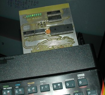
The board is commanded by two Z80 I/O ports - port 31 to change the selected flash ROM memory page (and map in and out the Spectrum's ROM), and port 63 to light up the LEDs. To describe how this actually works on the hardware level, we'll start from the address decoding and work inwards from there.
When the Z80 CPU executes an IN or OUT instruction, the following things happen. Firstly, the Z80 places the I/O port address on the address bus - for the instruction OUT (63), A - the lower 7 bits of the address bus are set to 63 (3F in hex). Then the /IORQ line goes active (low voltage level), and the /WR line goes active (also logic low).
The board senses an OUT instruction with the chip U1 - a 74HC138. This is a 3-to-8 line decoder. Address lines A5, A6 and A7 are connected to the three address lines on the '138. You can count from 0 to 7 with three binary bits, and what the '138 does is activate output 0 to 7 depending on what 3 bit number arrives on its inputs. So really - what's important is what the Z80's address lines A5, A6 and A7 are outputting during an I/O cycle. We're only using 2 outputs on this chip - output 0 for the memory bank selection, and output 1. So if the pattern on A5, A6, A7 from the Z80 is 000, then the memory is selected. If the pattern on these three address lines is 001, then the LED register is selected.
As well as the right pattern being on the address bus, we've got to be able to determine that the Z80 is making an I/O request, and not a memory request or an interrupt acknowledge. The '138 has three Enable pins for this purpose. Indeed, it doesn't matter what the state is on the three address pins on this chip if the enable pins aren't set to the right levels - all outputs will remain inactive. To tell whether the Z80 is making an I/O request, two pins must be monitored - IORQ and M1. IORQ must be low and M1 must be high. (Why must M1 be monitored? This is because the Z80 acknowledges a maskable interrupt by a special M1 cycle, with IORQ low and M1 low. Spurious address decodes can occur if only IORQ is used for an enable). Additionally, we also look at the state of WR to make sure we're getting an OUT instruction, not an IN instruction, since this board only requires I/O writes and not reads.
Of course, it would be simple if large numbers of Spectrums hadn't shipped with Z80s with faulty M1 lines. A faulty M1 line doesn't seem to affect a Spectrum at all if it's used stand alone, but it can stop some peripherals from working properly. Therefore, a jumper is provided on the board to ignore M1, so that the I/O decoding relies just on IORQ and WR being active together (which is also only the case during an OUT instruction, not an interrupt acknowledge). If you change the jumper so that M1 is used, you can write a short BASIC program to test the functioning of M1:
10 OUT 63, 255
20 PAUSE 5
30 OUT 63, 0
40 PAUSE 5
50 GO TO 10
If the LEDs all rapidly blink on and off in a stable and consistent manner, M1 works. However, if the blinking is somewhat erratic, then M1 is faulty.
So all being well, the 74HC138 looks for an instruction for the board by monitoring the state of IORQ, WR and M1 to recognise an I/O write instruction, and uses the state of A5, A6 and A7 to select either the memory page register or the LED register. The output of the '138 goes low when it's selected.
The 74HC273 is not level triggered - rather, it latches the contents of the data bus on the rising edge of the signal on the CP pin. When the Z80 de-asserts IORQ, the active low output of the 74HC138 will return high. The Z80 keeps the contents of the address bus live for about half a clock cycle after it has de-asserted IORQ - this is to allow edge triggered devices to read the contents of the data bus without needing any additional glue logic. This timing means the rising edge of the 74HC138's output can be used to latch the value being sent by the OUT instruction that's running on the CPU.
The 74HC273 octal flip flop, U5, performs the function of being the memory page register. The board can take flash ROMs from 128K to 512K, which is far larger than the address space that a Z80 can access. Therefore, this chip controls the state of address lines A14 to A18 on the flash memory. This chip also has a reset pin, so on power up or when the reset button is pressed, A14 to A18 are all at logic low, so the first 16K page of ROM is selected. Additionally, bit 5 of this chip is used to control whether the Spectrum's ROM is paged in, or whether the flash is paged in. The Spectrum provides a line called ROMCS at the edge connector. There is a resistor between the ULA's ROM chip select decoding logic and the ROM itself, and ROMCS is connected on the ROM's side of this resistor. Since the Spectrum's ROM is enabled when ROMCS is low, holding this line high will prevent it from being selected.
This is accomplished on the diagnostics board by bit 5 of the rom page register U5 being connected to the gate of a P-channel MOSFET. The MOSFET connects the +5v line to ROMCS when it is turned on. It is turned on by bit 5 of U5 being set to logic low with the jumper on J1 on pins 1 and 2. If the jumper on J1 is on pins 2 and 3, the output of bit 5 is inverted before being sent to the gate of this transistor, which means bit 5 needs to be set to logic 1 for the flash to be paged in.
This allows the board also to be used as a general purpose ROM board, so that different ROMs can be paged in at will. Also, programs can be written to copy a program to RAM, for example, a snapshot taken on an emulator and written to the flash chip.