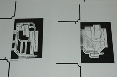
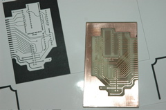
Making a PCB for the LCD interface - laser printed onto gloss photo paper. Top of PCB is left, solder side is right. A two layer board :-)
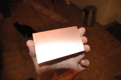
A piece of double sided copper clad board cut off a larger piece
The PCB design ironed on with a clothes iron. The toner bonds to the copper and acts as etch resist.
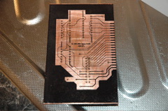
The toner cleaned off, and the board drilled. The registration was good and the copper matched up on both sides for all the vias and pin holes.
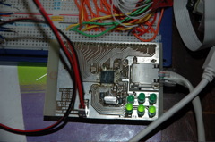
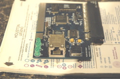
W5100 breakout board connected to ALIAC-2, showing FDX, LINK and 100Mbps lights.
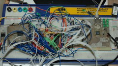
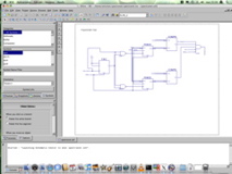
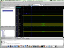
General view of the scene