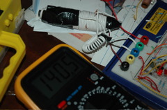
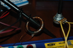
Home made inductor for the buck converter - multimeter showing just over 140 volts.
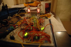
Nixie lit up - decimal point and the digit 6. (Just visible in the out of focus foreground - LED off 555 timer and power transistor providing the switch in the buck converter)
Nixie with 6 and decimal point illuminated
More turns added to the inductor, increasing the voltage to 148 volts
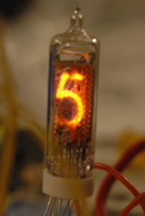
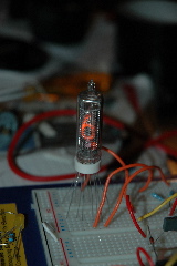
Not quite completely illuminated 5
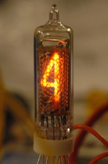
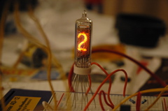
Well illuminated 4
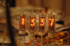
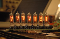
Four tubes running - 155 volts, 33k ohm series resistors
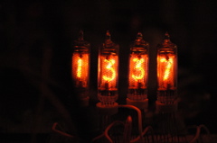
Four tubes running
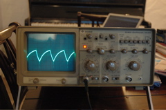
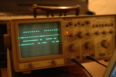
The 'scope has arrived! The trace is showing what the capacitor connected to the 555 timer is doing.
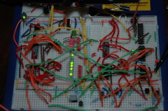
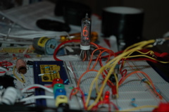
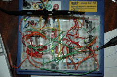
Perhaps the electronic equivalent of spaghetti code...
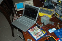
The ...um... workbench. Well, the dining room table has been pressed into service as the workbench.
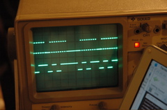
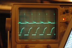
Register clock pulses on the top trace, RS232 data (after passing through the MAX233) on the bottom.
The final prototype (spot the changes)
More data goes by (the bottom trace - the output from the MAX233CPP IC looks odd due to the long camera exposure)
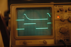
Top trace is the pulse generator's output, being repeatedly driven by a 555. This is the waveform with the PNP transistor and version 1 of the circuit. Version 2 has a much steeper drop off, and version 3 is practically square wave.
Low speed testing of the serial sender. The MAX233 isn't yet connected.
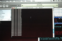
Yay! Data successfully being sent to the computer!
The circuit, now set up to send 0xFF to the VAX. 10 ICs just to send one byte :-)
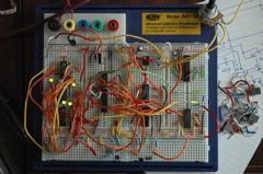
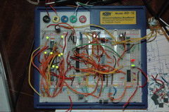
Left 2 ICs: 4043 latches. Top middle ICs - 4050 buffers. Bottom middle - first K155ID1, right middle upper - 555 based switch mode boost converter, bottom right middle, second K155ID1. Right most are the nixies.
Top waveform - what the inductor is doing. Bottom waveform - input to the switching MOSFET
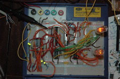
Ummm. Yeah. Well. Foreground - two 4043 latches (LEDs show binary state - 0x6 and 0x9), mid picture - two 4050 buffers and the first K155ID1, middle background - switch mode supply and second K155ID1. Finally, the nixies.
My second revision of home made inductors - proper inductor wire this time. The scope probe shows what's happening without needing to be actually connected.
I wonder why I've not tried sleeping here before!
Nice and warm with a conveniently comfortable upslope...
Smudge: Displaying '69' on those nixies is not big and it's not funny!
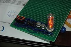
First digit and its driver soldered in. The socket in the back has some test wiring to give an input to the K155ID1
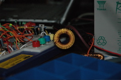
The new, manufactured 150uH inductor works much better for the 170v switch mode power supply.
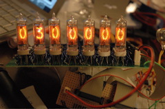
All nixies on the board! Some test numbers being shown - the first 4 driven via the K155ID1s, the last three with some test jumpers. Numbers getting a bit dim because my lead acid battery is getting a bit low and the SMPS can't quite make 170v off its output.
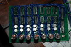
Looking down on the board. Top sockets are for 4050 CMOS buffers, bottom sockets for K155ID1s, silver components are the 2N3440 transistors, and at the bottom are of course the tubes. A little more wiring needed to finish off.
Performing a 'sniff test' of the completed board - number sequence statically wired into the breadboard.