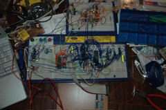
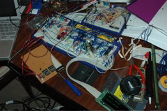
A proto-computer. Top breadboard: RS232 decoder. Bottom perfboard: 16 bit counter with tri state outputs. Main breadboard: left - chip select logic, middle left - AMD Am29F010B flash ROM, middle right - buried under blue wire - 2K Toshiba static RAM, to its right the Z80. Rightmost, simple output device with 8 LEDs.
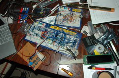
Simple output device replaced with the Z80 PIO (rightmost). We can take input!
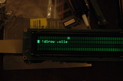
Not quite what I was hoping for!
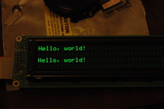
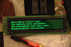
That's better! The display actually works as two halves - there's a controller for the top two and top bottom two lines. The program tests both.
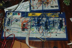
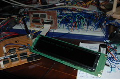
The ever growing tangle of wires. The PIO is the right most 40 pin chip, connected to the LCD.
LCD interface designed, assembled and coded for - all four lines in use - so both LCD controllers being selected sequentially.
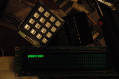
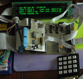
The keypad works! The computer now has both input and output interfaces with humankind.
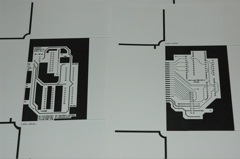
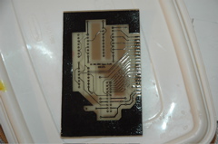
Making a PCB for the LCD interface - laser printed onto gloss photo paper. Top of PCB is left, solder side is right. A two layer board :-)
Using a halogen light behind the paper to get the registration right (i.e. make the holes on both sides of the PCB match up)
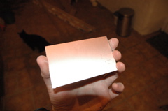
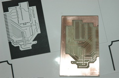
A piece of double sided copper clad board cut off a larger piece
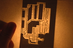
The PCB design ironed on with a clothes iron. The toner bonds to the copper and acts as etch resist.
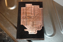
After etching and washing. Copper gone, but toner still in place.
The toner cleaned off, and the board drilled. The registration was good and the copper matched up on both sides for all the vias and pin holes.
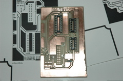
Vias soldered, chip sockets added plus a resistor (waiting on a 1mm drill bit for the connectors)
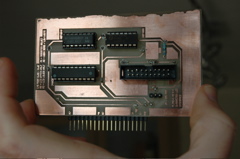
The finished PCB. At this stage I had also done a sanity check on the board (giving it power and manually setting logic signals and checking the output on the IDC connector)
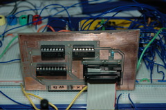
The board now plugged in, freeing up space on the breadboard for more experiments.
A view of the breadboard
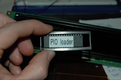
Backup ROM just in case! The 'umbilical cord' of the raw logic serial loader has been removed, the machine must now stand on its own two feet and load data via PIO port A.
The printed circuit board, warts and all! Left to right - top row, Z80 CPU, 74HC32 quad OR gate, 74HC14 inverter, 74HC138 decoder, Z80 CTC. Bottom: 32K SRAM, 128K flash ROM, 74HC574 flip flop (ROM page selector), Z80 PIO.
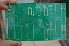
Board fresh in from Olimex
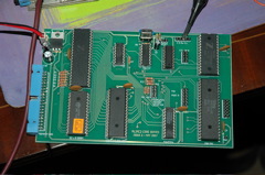
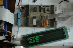
The board from Olimex populated, and running a test routine (with the scope connected to the I/O port decoder to show the test running)